
nextnano
Simulation of Electronics and Optoelectronics, Semiconductor Devices with Quantum Physics
무어의 법칙을 기반으로 한 실리콘 기반 반도체 소자의 집적화는 끊임없이 반도체 소자의 크기를 더 작게 만드는데 기여하고 있습니다. 수나노 이하의
소자 크기가 현실화됨에 따라 원자간 상호 작용의 영향력을 고려한 원자 단위 수준의 모델링 접근법이 필수적인 상황입니다. 따라서 전자의 파동성을
고려한 슈뢰딩거 방정식 기반의 양자역학 시뮬레이션을 수행하지 않는다면, 소자 특성의 계산은 더 이상 그 결과를 신뢰할 수 없습니다.
nextnano는 사용자가 모델링한 임의의 구조를 대상으로 기본적인 반도체 및 화합물 반도체의 물성을 정확히 반영한 양자역학 시뮬레이션을 수행합니다.
Schrödinger-Poisson-Current Solver를 활용해 양자역학을 고려한 전기적 특성을 계산함으로써 Quantum dot/well/wire, Laser Diode, VCSEL,
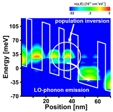
Quantum Cascade Laser 등의 광전자 소자와 더불어 High Electron Mobility(HEMT), Rapid Diode Tunneling(RDT) 등 나노스케일 반도체 소자의 물리적
특성을 정확하게 예측할 수 있습니다.
특징 및 기능
Advanced Quantum Physical Solver
- 8 band k.p model quantum transport solver
- Schrödinger-Poisson-Current solver
- Nonequiliribrium Green s Function(NEGF) quantum transport solver
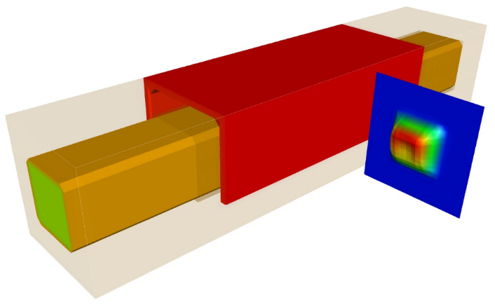
Epitaxially Grown Heterostructure Modeling
- Materials: Group lV, lll-V, ll-VI (Zinc blende, Wurtzite)
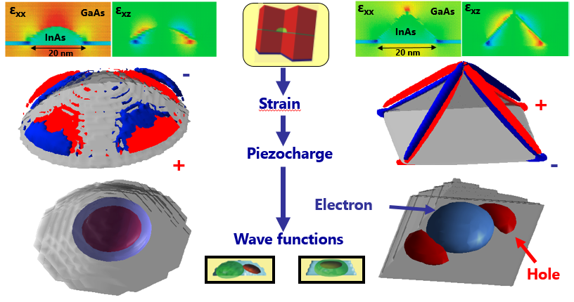
- Includes Strain, Piezo and Pyroelectricity
- Growth directions along [001], [011], [111],... in short along any crystallographic direction
Accurate Prediction of Physical Properties
- Electron wavefunctions
- Energy band diagram
- Electron density
- Local density of states
- Optical gain
Research Group License
- nextnano는 대학 및 연구기관에 한해 연구 그룹별로 라이선스를 제공합니다. 한 개 라이선스 구매로 소속 그룹의 인원들이 모두 nextnano를 사용할 수 있습니다.
응용분야
nextnano는 나노스케일 반도체 소자의 전기적 특성을 예측하기 위한 목적으로 범용적으로 사용할 수 있습니다.
관심 갖고 계신 분야의 튜토리얼(nextnano Tutorials)을 검색하신 다음, 평가판 사용을 통해 직접 시뮬레이션 결과를 확인해 보시기 바랍니다.
.
- MOSFET
- Strained Silicon
- HEMT
- RDT
- Quantum Cascade Laser
- Quantum well,dot,wire
- Superlattices
- Type-ll heterostructures
- Laser diode
- VCSEL